Showing posts with label Electronic projects. Show all posts

Sunday, September 1, 2013

Alcohol Breathalyzer circuit using 8051 microcontroller (AT89S51).

This article is about a breathalyzer circuit using 8051 microcontroller which outputs the blood alcohol content (BAC) from the breath. The BAC is displayed in percentage on a 3 digit seven segment display. The microcontroller used if AT89S51 which belongs to the 8051 family and the alcohol sensor is MQ135 gas sensor from Futurelec.

MQ135 gas sensor.

MQ135 is a stable and sensitive gas sensor which can detect  ammonia, carbon dioxide, alcohol, smoke, nitrogen dioxide etc. The sensor consists of a tin dioxide sensitive layer inside aluminium oxide micro tubes, measuring electrode and a heating element inside a tubular aluminium casing. The front end of the sensor is covered using a stainless steel net and  the rear side holds the connection terminals.
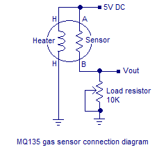
The ethyl alcohol present in the breath is oxidized into acetic acid while passing over the heating element. This ethyl alcohol falls on the  tin dioxide sensing layer and as a result its resistance decreases. This resistance variation  is converted into a suitable voltage variation using an external load resistor. The typical connection arrangement of an MQ135 alcohol sensor is shown below.
mq135 alcohol sensor
MQ135 alcohol sensor
MQ135 has different resistance values at different temperature and different concentration of gases. The manufacturer recommends to calibrate the sensor at 100ppm of ammonia or 50ppm of alcohol. The recommended value of the load resistor is between 10K to 47K.

Circuit diagram.

Breathalyzer using 8051

The voltage output of the alcohol sensor is converted into a digital format using the ADC0804 (IC1). The Vref/2 pin of the ADC is held at 1.28V using the voltage divider network made of R14 and R15. Vref/2 =1.28V means the step size of the ADC will be 10mV and the output of the ADC will increment by one bit for every 10mV increment in the analog input. Refer the datasheet of ADC0804 for a better grasp. Digital out of the ADC (D0 to D7)  is interfaced to Port1 of the microcontroller. Control signals CS, RD, WR, INTR are obtained from the microcontrollers P3.7, P3.6, P3.5, P3.4 pins respectively. R9 and C1 are associated with the clock circuitry of the ADC0804.
Capacitor C3 connected between Vin+ and Vin- of the ADC0804 filters of noise (if any) in the sensor output. If C3 is not used the digital output of the ADC will not be stable. This filter capacitor will surely induce some lag in the ADC response but it is not very relevant in this entry level application. The microcontroller performs required manipulations on the ADC digital output in order to convert it into BAC % and displays it on the three digit seven segment display. Port0 of the microcontroller is interfaced to the multiplexed three digit seven segment display. The drive signals for the threes digits are obtained from the microcontroller’s P3.0, P3.1, P3.2 pins respectively.

Program.

ORG 00H
MOV P1,#11111111B
MOV P0,#00000000B
MOV P3,#00000000B
MOV DPTR,#LUT
MAIN: MOV R4,#250D
      CLR P3.7
      SETB P3.6
      CLR P3.5
      SETB P3.5
WAIT: JB P3.4,WAIT
      CLR P3.7
      CLR P3.6
      MOV A,P1
      MOV R5,A
      SUBB A,#86
      JC NEXT
      SETB P3.3
      CLR PSW.7
NEXT: MOV A,R5
      SUBB A,#115D
      JNC LABEL
      MOV A,#00000000B
      CLR PSW.7
LABEL: MOV B,#5D
       MUL AB
       MOV B,#8D
       DIV AB
       MOV B,#10D
       DIV AB
       MOV R6,A
       MOV R7,B
DLOOP:SETB P3.0
      MOV P0,#01000000B
      ACALL DELAY
      CLR P3.0
      SETB P3.1
      MOV A,R6
      ACALL DISPLAY
      MOV P0,A
      ACALL DELAY
      CLR P3.1
      SETB P3.2
      MOV A,R7
      ACALL DISPLAY
      MOV P0,A
      ACALL DELAY
      CLR P3.2
      DJNZ R4,DLOOP
      SJMP MAIN
DELAY: MOV R3,#255D
LABEL1: DJNZ R3,LABEL1
        RET
DISPLAY: MOVC A,@A+DPTR
         CPL A
         RET
LUT: DB 3FH
     DB 06H
     DB 5BH
     DB 4FH
     DB 66H
     DB 6DH
     DB 7DH
     DB 07H
     DB 7FH
     DB 6FH
END

Notes.

  • The MQ135 gas sensor requires around 5 minutes of preheat before the first use.
  • The MQ135 takes few minutes to retrace back to its normal condition after a positive test (alcohol present in the breath).
  • If there is no alcohol in the breath  the sensor output will swing back to its normal condition very fast.
  • Read these articles Interfacing seven segment display to 8051 microcontroller , Interfacing ADC to 8051 microcontroller  before attempting this project.
  • This breathalyzer circuit is just an entry level one and is not suitable for high end applications such as law enforcement or laboratory application.
  • The logic for converting the digital output of ADC into BAC percentage was obtained using approximation techniques.

Saturday, August 18, 2012

Automotive Telematics


A Prototypic Design Approach for Automotive Telematics On-board Unit Platform (ATOP) Using ARM Powered NFC (Near Field Communication) Technology


SYNOPSIS:
                In today’s fastest world the use of vehicle is unavoidable as well as the accident occurring due it is also a biggest issue.  So we have designed the system in a move to save lives on the road by measuring the pressure of the vehicle. Current estimates suggest annually there are around 43,000 deaths across Europe’s road networks. Experts believe this could be reduced significantly if the load of the vehicle is maintained as well as the traffic is also maintained by allowing the heavy vehicles only in the specific time.
PROBLEM STATEMENT:
•         Measuring the load and perimeters are crucial
•          Detection of the vehicle is difficult
•         Miscellaneous of  vehicle in the city for long durations

PROPOSED SYSTEM:
In this proposed system we have designed the system with three applications. First application is to calculate the strain of the vehicle. By using strain sensor, pressure of the vehicle is monitored. When the strain exceeds the set up value the information is suddenly passed to the RTO office through wireless technology. By using this application over loading of the vehicle can be avoided which may lead to an accident. So by using this system even if the owner tried to overload his vehicle he can’t do it. By using this system driver can drive his vehicle safely and accident freely.
In the second application traffic jam can be reduced by maintaining the specific time for heavy vehicle. Heavy vehicles should enter the city only at the specific time. If they entered at some other time information is transferred to the control room.
The third application is used to maintain the traffic signal properly. If any vehicle crosses the road when the signal is red .Then the vehicles id is passed to the nearest control room. Intruder sensor is used to detect whether the vehicle crosses the road in the proper way or not.

BLOCK DIAGRAM:
Vehicle section:


Control Room Section:


Signal Section:


REQUIREMENTS:
Hardware Requirements:
Ø  Microcontroller
Ø  RF module
Ø  Decoder/encoder
Ø  Pressure sensor
Software Requirements:
Ø  Keil IDE
Ø  Flash magic
Ø  ORCAD
Ø  Embedded C

APPLICATIONS:
•         Highly Reliable.
•         Traffic signal will be controlled
•         Automatic fine can be charged using wireless technology
•         Much more efficient than the existing system.
 

Thursday, August 16, 2012

Smart Car


SYNOPSIS:

In modern world, many new techniques such as biometric recognition technique, image processing technique, communication technique and so on, have been integrated into car security systems. At the same time, the amount of accident of cars still remains high, specially, lost. Traditional car security systems rely on many sensors and cost a lot. When one car is really lost, no more feedback could be valid to help people to find it back.

PROBLEM STATEMENT:
•       No information to the Owner if Car get Lost
•       Traditional car security systems rely on many sensors and cost a lot
•        Physical Key.
•       Alarm System

PROPOSED SYSTEM:

In proposed system we introduced a low-cost extendable framework for embedded smart car security system is proposed, which consists of a face detection subsystem(FDS), a GPS (Global Positioning System) module, a GSM (Global System for Mobile Communications) module and a control platform. The face detection technique to be applied in car security system because this kind of technique is effective and fast, and one alarm signal could be given to make an alarm or “call” the police and the host soundlessly with the help of other modules in the system prototype. Experimental results illuminate the validity of this car security system, and it is also much cheaper and ‘smarter’ than traditional ones.
FDS (face detection subsystem) is used to detect the face of the driver and compare it with the predefined face, for example, in the night when the car’s owner is sleeping and someone theft the car then FDS obtains images by one tiny web camera which can be hidden easily in somewhere in one car. FDS compares the obtained image with the predefined images if the image doesn’t match then the information is send to the owner through MMS. So now owner can obtain the image of the theft in his mobile as well as he can trace the location through GPS.  The location of the car as well as its speed can be displayed to the owner through SMS. So by using this system owner can identify the theft image as well as the location of the car.
Block Diagram:

Vehicle Section:


HARDWARE REQUIREMENTS:
•      Microcontroller
•      Power supply
•      Keypad section
•      GSM module
•      Web Camera
•      Ignition unit | Driver unit

SOFTWARE REQUIREMENTS:
•      Keil C cross compiler IDE
•      Flash magic programmer tool
•      Orcad hardware design tool
•      Visual basic 6.0
•      Matlab7.5
•      Languages:
–     Embedded C
–     Visual Basic

APPLICATIONS:
•      Security applications
•      Image processing applications
•      Banking applications

Wednesday, August 15, 2012

HEAD INTERFACE SYSTEM


Abstract
The head interface system (HIS) consists of a tablet model device in which the operations on it can be performed by interfacing the movements of our head. The main part of the system is a tablet computer like device of which the mouse pointer can be controlled by the movements of our head. So physically handicapped people can use this device for several purposes. The device has several features in it. Some the features are that it can share video files with a television set through wireless media, It can share sound files with a music system or a speaker , Functions as a television remote. It can control all household electrical devices such as light, fan, air conditioner, water pump, It can access security cameras, it can control a mini robot or a wheel chair with motors . Also it can interface with pc. These features are achieved by the Bluetooth modules in the device and also there should be Bluetooth modules attached with those devices that we want to control with the HIS system.


Block Diagram


Processor: Arm processor development board

Challenges in this project


·         To invent a system to sense the movements of head
·         To build a tablet like device with a processor and display
·         Programming the device
·         To interface various devices

Device controlling with remote

Description
 In this project a circuit is designed to control any four electrical devices such as fan,light,television etc. with a small remote. The size of the remote is so small such that you can made it look like a key chain.


BLOCK DIAGRAM EXPLANATION


VOLTAGE REGULATOR
            The IC is used as the voltage regulator. It converts the 6V supply into 5V regulated supply
ENCODER
          The IC HT12E is used as the encoder. It converts the input pulse into binary signals and it is given to the transmitter..
ASK TRANSMITTER
            The ASK transmitter is a 433 MHz Radio Frequency signal transmitter. ASK is short for Amplitude Shift Keying. It modulates the binary signals into analogue signal.
ASK RECEIVER
The ASK receiver receives the binary signals transmitted by the transmitter. It demodulates the received analogue signal into binary signal.
DECODER
The IC HT12Dis used as decoder. It decodes the binary signal.

 CIRCUIT  DIAGRAM

remote section


 Receiver section


WORKING
           

This device has two circuits, one for the remote section and other for controlling devices. The basic working of the robot is that, when the switch in remote is pressed then a signal is produced and it is then encoded and then modulated and transmitted to the recever and the receiving section demodulate and decodes the signal and the signal in remote is reproduced in the receiving unit. This signal is applied to the relays

Here we use HT12E and HT12D as the encoder and decoder. They have 8 bit address and 4 bit data. Hence we can transmit 4 signals , using theses 4 signals we can control 4 devices
Now consider the remote section .The main elements in the remote section are an encoder IC, an ASK transmitter and four switches. The encoder IC has 18 pins. The pins one to eight are the address bits. The four pins, pin no.8 to 13 are the data bits or input terminals. These four pins are connected to the four switches. When a switch is closed, that pin is grounded. Thus a signal is produced and the encoder converts it into binary signal and this binary signal is modulated and transmitted by the ASK transmitter.

Now consider the receiver section. The signal is received and demodulated by the ASK receiver and this binary signal is given to the decoder. The decoder converts it into actual signal corresponding to the pin in encoder, the same pin produces a ground signal while the other data pins produces a +VCC as output. The output from the data pins are given to the relays.


Tuesday, August 14, 2012

Fm Transmitter Hunt aka Fox Hunt


      Fox hunt aka fm transmitter hunt is game where the mission is to find the fm transmitters which hidden from the players. The principle used here is the fm transmitters are hidden and they will transmit a melody continuously. The players are provided with fm receivers consisting of Directional ( yagi uda) antennas. By using these directional antennas the locations of the hidden transmitters can be found. There will be more than 4 or 5 transmitters, those who found the maximum number of transmitters will win the competition.

Transmitter section


Description

Here is a simple melody generator circuit you can make using an IC, it is combined with a fm modulator.The  UM66 series are CMOS IC’s  designed for using in calling bell, phone and toys. It has a built in ROM programmed for playing music. The device has very low power consumption.Thanks for the CMOS technology.The melody will be available at pin3 of UM66 and here it is amplified by using Q1 to drive the speaker.Resistor R1 limits the base current of Q1 within the safe values.Capacitor C1 is meant for noise suppression.


       Circuit showing a fm transmitter.Here i have used a bc494 high frequency transistor for making this circuit .The fm modulator is changing the frequency of carrier signal according to the strength of information signal


Component Required
  1. Resistor   :39k.100R
  2. Capacitor  :10MF,2.2PF,4.7PF-2,102PF,103PF, 0.1uf,
  3. Transistor: BC 494, HE8050S
  4. Inductor :22nH
  5. IC : um66

 Receiver Section

Description

                  Circuit showing a fm radio receiver .Here i have used ic cxa1619bs for making this circuit.Construct this circuit on a good pcb and give me your comment. The yagi uda antenna will provide high directivity.Part list and applications are showing below


Part List

Component No:    Value    Usage
R1    220R    Noise Reduction
R2    150R    Crystal Grounding
R3    330R  
R4    330R  
R5    330R,1/2 W      Current Limiting
C1    22pF    Oscillation
C2    22pF    Oscillation
C3    22pF    Oscillation
C4    203pF  
C5    102pF  
C6    4.7MF    Noise Grounding
C7    47pF    Feedback
C8    203pF    Noise Grounding
C9    100MF    Decoupling
C10    4.7pF    Voice Noise Grounding
C11    104pF    Audio Coupling
L1    22nH,3T    Oscillation
L2    22nH,4T    Oscillation
L3    22nH,5T    Oscillation
X1    4.7MHz    IF Frequency Generator
X2    2.7MHz    Mixer Frequency Generator
VC1    27pF Gang    Tuning
U1    CXA1619BS     Main IC

Antenna Design


 FOX HUNT competition in our college

USB Power Jukebox


Thanks :This project was designed by one of our readers " Mr. Sreenath C J".......


INTRODUCTION

This is a USB Power jukebox system without microcontroller.
In this project a USB player has been attached for music enhancement from pen drives/memory cards. It gives lot of comfort to the user since we can operate it at the time of power failure. We can also charge USB power devices/Phones and provides output DC voltages.
In this project consist of 3 sections, Mini ups system, USB power socket and USB audio player and USB power jukebox is a portable system.


BLOCK DIAGRAM


BLOCK DIAGRAM DESCRIPTION


           Standard step down transformer provides 12V of AC used in this circuit. AC output of transformer connected to mini ups circuit. The mini ups circuit provides an uninterrupted power supply to operate 12V, 9V, and 5V DC-powered instruments at up to 1A current. This circuit consists of   LED’s, diodes, zener diodes, battery, resistors & capacitors. The circuit immediately disconnects the load when the battery voltage reduces to 10.5V to prevent deep discharge of the battery. The capacitor C1 provides ripple-free DC to charge the battery.
         The output of mini ups system connected to USB power socket & USB player. Nowadays, many handheld devices utilizes this facility of USB port recharge their built-in battery pack with the help of an internal circuitry. Usually 5V DC, 100mA current is required to satisfy the input power demand.

USB AUDIO PLAYER MODULE


                  USB Player module consists of USB/Memory card slot and music modes or functions can be operated by a remote. It  operates on  5V,250ma DC supply.


CIRCUIT DIAGRAM


MINI UPS SYSTEM


Fig-1

USB POWER SOCKET


Fig-2


CIRCUIT DIAGRAM DISCRIPTION


MINI UPS SYSTEM


       This circuit provides an uninterrupted power supply (UPS) to operate 12V, 9V and 5V DC- powered instruments at up to 1A current. The backup battery takes up the load without spikes or delay when the mains power gets interrupted. It can also be used as a workbench power supply that provides 12V, 9V and 5V operating voltages. The circuit immediately disconnects the load when the battery voltage reduces to10.5V to prevent deep discharge of the battery. LED1 indication is provided to show the full charge voltage level of the battery. Miniature white LEDs (LED2 and LED3) are used as emergency lamps during power failure at night.

        A standard step-down transformer provides 12V of AC, which is rectified by diodes D1 and D2. Capacitor C1 provides ripple –free DC to charge the battery and to the remaining circuit. When the main power is on, diode D3 gets forward biased to charge the battery. Resistor R1 limits the charging current. Potentiometer VR1 (10K) with transistor T1 acts as the voltage comparator to indicate voltage level. VR1 is so adjusted that LED1 is in the ‘off’ mode. When the battery is fully charged, LED1 glows indicating a full voltage level of 12V.

       When the mains power fails, diode D3 gets reverse biased and D4 gets forward biased so that the battery can automatically take up the load without any delay. When the battery voltage or input voltage falls below 10.5V, cut-off circuit is used to prevent deep discharging of the battery. Resistor R3, zener diode ZD1 (10.5V) and transistor T2 from the cut-off circuit. When the voltage level is above 10.5V transistor T2 conducts and its base becomes negative (as set by R3, VR2 and ZD1). But when the voltage reduce 10.5V, the zener diode stops conduction and the base voltage of transistor T2 becomes positive. It goes into the ‘cut-off’ mode and prevents the current in the output stage. Preset VR2 (22k) adjust the voltage 0.6V to make T2 work if the voltage is above 10.5V.


        When power from the mains is available, all output voltages-12V, 9V and 5V-are ready to run the load. On the other hand, when the mains power is down, output voltages can run the load only when the battery is fully charged (indicated by LED1). For the partially charged battery, only 9V and 5V are available. Also, no output is available when the voltage goes below 10.5V. if battery voltage varies between 10.5V and 13V, output at terminal A may also vary between 10.5V and 12V, when the ups system is in battery mode.

      Outputs at points B and C provides 9V and 5V, respectively, through regulator ICs (IC1 and IC2) while output A provides 12V through the zener diode. The emergency lamp uses two ultra-bright white LEDs (LED2 and LED3) with current limiting resistors R5 and R6. the lamp can be manually switched ‘on’ and ‘off’ by S1.

       The circuit is assembled on a general-purpose PCB. There is adequate space between the components to avoid overlapping. Heat sinks for transistor T2 and regulator ICs (7809 and 7805) to dissipate heat are used.
The positive and negative rails should be strong enough to handle high current. Before connecting the circuit to the battery and transformer, connect to a variable power supply. Provide 12V DC and adjust VR1 till LED1 glows. After setting the high voltage level, reduce the voltage to 10.5V and adjust VR2 till the output trips off. After the settings are complete, remove the variable power supply and connect a fully-charged battery to the terminals and see that LED1 is on. After making all the adjustments connect the circuit to the battery and transformer. The battery used in the circuit is a 12V, 4.5Ah UPS battery.


USB POWER SOCKET


       A USB port, in practice is a capable of delivering more than 100mA of continuous current at 5V to the peripherals that are connected to the bus. So a USB port can be used, without any trouble, for powering 5V DC operated tiny electronic gadgets.


       Nowadays, many handheld devices (for instance, portable reading lamps) utilize this facility of the USB port to recharge their built-in battery pack with the help of an internal circuitry. Usually 5V DC, 100mA current is required to satisfy the input power demand.
Fig. shows the circuit of a versatile USB power socket that safely converts the 12V battery voltage into stable5V.This circuit makes it possible to power/recharge any USB power-operated device, using in-dash board cigar lighter socket of your car.


       The DC supply available from the cigar lighter socket is fed to an adjustable, three-pin regulator LM317L (IC1).capacitor C1 buffers any disorder in the input supply. Resistors R1 and regulate the output of IC1 to steady 5V,
Which is available at the ‘A type female USB socket. Red LED1 indicates the output and zener diode ZD1acts as a protector against high voltage.


PCB LAYOUT


MINI UPS SECTION


FIG-1


USB POWER SECTION


FIG-2


POWER SUPPLY UNIT


                   All electronics words only with low DC voltage. We need a power supply unit to provide the appropriate voltage supply. In this project a Dc voltage source of 12V is used to run and charge the circuit and regulator IC (7405, 7409) is used provide regulated 5V and 9V supply.


PCB FABRICATION

The PCB fabrication involves the following steps

1. PREPARATION OF THE LAYOUT

       First the circuit is drawn in orcad capture and the layout is prepared by the orcad layout plus as explained in the layout making procedure. From the layout plus the mirrored image of the top layer is printed on the butter paper. Using this, the film can be made and is exposed to the UV. 

2. FILM PREPARATION

        In this process, the negative of the film is made on photogenic film. For this, the printed image of the layout in butter paper is placed over the film and it is exposed to the UV rays from the top so that the film will be exposed to the UV rays in the regions other than the layout. Then the developer solution is made and the film is taken out of the exposure unit and is put in the developer solutions, then the reaction will take place, then the regions not exposed by UV rays will become transparent and the other regions are dark in color. Thus the negative is produced. Then the film is washed in fixing solutions. After that the film is kept for drying.

3. TRANSFERRING OF THE LAYOUT TO COPPER CLAD

          First the copper clad sheet of required size is cut by using cutting machine. Then the sheet is cleaned by using steel scrubber. After perfect cleaning of the board, it is dipped in the photo resist solution so that film of the photo resist is formed on the board. Then the copper clad sheets placed in an oven for sometime, so that the photo resist will fixed to the surface of the board.

           The next step is to form an image of the layout on the copper clad sheet. For that, the negative of the layout is placed over the sheet. Then it is placed on the UV exposure unit so that the UV rays will fall on the photo resist over the board in the regions of the layout where the negative is transparent. Then the board is taken out and put in a developer solution for about 1.15 minutes. After that, the board is washed gently in water for about one minutes so that the chemical reaction take place in the regions exposed by the UV rays. Then the board is washed in a dye so that the dye will be fixed to the layout regions. Thus we get the visible image of the layout on the board. Then check the layout on the board with the actual circuit. If any mistakes, the above processes are repeated. If layout is correct, the board now ready for etching.


4. ETCHING OF THE LAYOUT

         When the board is ready for etching it is placed in the ferric chloride solution. It is checked in regular intervals to prevent over etching and successive damage to the port. After the etching is complete, the board is taken out of the etch and washed in water to remove the excess ferric chloride. Now the copper lines are exposed and hence the body is checked with the magnifying glass to see whether all the lines in the layout are clearly formed now the board is ready for tinning.

5. TINNING

         For tinning, the PCB is cleaned well and the flux is supplied to the surface then it is passed through the tinning machine. In tinning the copper lines are platted with an alloy of TIN & LEAD.

6. DRILLING

         After tinning, the next process is drilling. In this the holes of required sizes are drilled in the PCB wherever needed, using an electrical drilling machine.
SOLDERING

           Soldering is the process of joining two or more similar or dissimilar metals by melting another metal having low melting point.

SOLDERING FLUXES

            In order to make the surface accept the solder readily the component terminals should be free from oxides and other obstructing films. Soldering flux cleans the oxides from the metal. The leads should be cleaned chemically or by scrapping using a blade or a knife. Small amount of lead should be coated on the cleaned position of the leads and the bit of the soldering iron. This process is called TINNING. Zinc chloride, ammonium chloride and rosin are the most commonly used fixes. These are available in petroleum jelly as paste flux. The residues which remain after the soldering may be washed out with more water accompanied by brushing.

SOLDER

              Solder is for joining two or more metals at temperatures below there melting point. The popularly used solders are the alloys of TIN(60%) and LEAD(40%) that melt at 375 deg Fahrenheit and solidifies when it cools. Most of the soldering wires are flux cored type. When such solder wires are used extra soldering flux is not required.      


SOLDERING TOOLS

SOLDERING IRON

               It is the tool used to melt the solder and apply at the joints in the circuit. It operates in 230V mains supply. The normal ratings of the soldering iron are 10W, 25W, 35W, 65W and 125W. the iron bit at the tip of it gets heated up with in a few minutes. 10W and 25W soldering irons are sufficient for light duty works.
Soldering gun: it is a gun shaped soldering tools used especially when more heat is required. Its trigger is a switch which controls the ac power.
Soldering station is an equipment which provides an iron and a control console that controls the temperature. The tip temperature is maintained by a feed back control loop.

DESOLDERING

              It is the removal or solder from a previously soldered joint. Desolder pump is a commonly used device for this purpose. When the solder melts by the action of the soldering iron, a trigger on the desolder pump should be activated to create a vacuum. This vaccum pulls the solder into the tube. 


COMPONENTS PRICE LIST


COMPONENTS                                                              PRICE  

BATTERY                                                                             450

TRANSFORMER                                                                    60        

LM317                                                                                      12

7805                                                                                          10

USB MODULE                                                                      450

TIP127                                                                                      15

LM3914                                                                                    55                                                            

LOUD SPEAKER                                                                    25

VOLTAGE REGULATOR (7805, 7809)                                10


APPLICATIONS

- It can be used for charging mobile phones, iPods etc

- Constant DC Outputs for DC powered devices

- Supports SD/MMC/MS cards for music enhancements


ADVANTAGES  


ADVANTAGES


- Backup upto 24hours.

-  Portable system


LIMITATIONS


- Only certain phone supports USB charging


FUTURE SCOPE


-          Small scale USB powered electronic devices can be operated by this system.
-          USB audio player can compatible with other audio devices ,amplifiers etc
-          Upcoming new i-pods requires USB charging


CONCLUSION


                         One of the primary objectives of an engineer is to endeavor to deliver best product or most efficient service at the lowest cost to the end user. System has been tested and was found to meet the expected result.
                   
                         Aim of this project is to design and construct USB power jukebox device. We have accomplished our aim and were successful in creating the device.


BIBLOGRAPHY


-          http://www.circuitstoday.com
-          http://www.electronicsforu.com